# The NVIDIA H100 GPU

The H100 is a <mark style="color:blue;">**graphics processing unit (GPU)**</mark> chip manufactured by Nvidia.&#x20;

It is currently the most powerful GPU chip on the market and is designed specifically for artificial intelligence (AI) applications.   <mark style="color:yellow;">**Each chip costs around $US75,000**</mark>.

The H100 is currently in high demand due to its powerful performance and its ability to accelerate AI applications.&#x20;

{% embed url="<https://www.youtube.com/watch?t=869s&v=MC223HlPdK0>" %}
This bloke just loves H-100s - a good review
{% endembed %}

### <mark style="color:purple;">Technological Foundations and Architecture</mark>

### <mark style="color:green;">Hopper Architecture</mark>

The H-100 is built around the <mark style="color:blue;">**Hopper architecture**</mark> - the latest GPU architecture developed by NVIDIA, named after the renowned computer scientist Grace Hopper.&#x20;

It succeeds the previous <mark style="color:blue;">**Ampere architecture**</mark> and introduces various improvements and new features to enhance performance and efficiency.

The Hopper architecture represents a lift in GPU technology, enabling faster processing, improved memory bandwidth, and more advanced features compared to its predecessor.&#x20;

It lays the foundation for the H100 GPU to deliver exceptional performance across a wide range of AI, high performance computing, and data analytics workloads.

<figure><img src="https://1839612753-files.gitbook.io/~/files/v0/b/gitbook-x-prod.appspot.com/o/spaces%2FpV8SlQaC976K9PPsjApL%2Fuploads%2FReuAXJbjAsa357SOc8tf%2Fimage.png?alt=media&#x26;token=3e9f90ea-27a0-46a6-9709-05395a2fcc2e" alt=""><figcaption><p>H100 FP16 Tensor Core has 3x throughput compared to A100 FP16 Tensor Core</p></figcaption></figure>

### <mark style="color:green;">TSMC's Custom 4N Process</mark>

<mark style="color:blue;">**TSMC (Taiwan Semiconductor Manufacturing Company)**</mark> is a leading semiconductor foundry that manufactures chips for various companies, including NVIDIA.&#x20;

The <mark style="color:yellow;">**custom 4N process**</mark> is a specialised manufacturing process developed by TSMC specifically for NVIDIA's H100 GPU, optimised for high performance and energy efficiency.

The custom 4N process allows NVIDIA to *<mark style="color:yellow;">**pack more transistors into a smaller area**</mark>*, enabling higher clock speeds and improved power efficiency compared to previous manufacturing processes.&#x20;

This advanced process technology is critical for achieving the H100's performance.

<figure><img src="https://1839612753-files.gitbook.io/~/files/v0/b/gitbook-x-prod.appspot.com/o/spaces%2FpV8SlQaC976K9PPsjApL%2Fuploads%2F7yHKJy84WI4WpbvA33wg%2Fimage.png?alt=media&#x26;token=2b593643-b2dc-43b1-a00e-072509c9ec2d" alt=""><figcaption><p>Taiwan is home to more than 90% of the manufacturing capacity for the world’s most advanced semiconductors.. Pictured here is a TSMC building in Taiwan</p></figcaption></figure>

### <mark style="color:green;">**Transistor Count and Die Size**</mark>

<mark style="color:blue;">**Transistors**</mark> are the basic building blocks of modern electronics, and the number of transistors on a chip is a key indicator of its complexity and potential performance. The <mark style="color:blue;">**die size**</mark> refers to the physical dimensions of the chip.

The H100 GPU features an astonishing <mark style="color:yellow;">**80 billion transistors**</mark>, which is a massive increase compared to the previous generation A100 GPU, which had <mark style="color:yellow;">**54.2 billion transistors**</mark>.&#x20;

To put this into perspective, the H100's transistor count is more than the combined population of several countries.&#x20;

The large <mark style="color:yellow;">**814 mm² die size**</mark> enables the integration of more processing units and memory interfaces, contributing to the H100's exceptional performance.

### <mark style="color:green;">**Streaming Multiprocessors (SMs)**</mark>

SMs are the primary processing units within an NVIDIA GPU, responsible for <mark style="color:yellow;">**executing parallel threads**</mark> and performing complex computations.&#x20;

<mark style="color:blue;">**SMs (Streaming Multiprocessors)**</mark> are the fundamental processing units that perform the parallel computations. They are similar to the cores in a CPU, but are designed specifically for parallel processing.

SMs are <mark style="color:yellow;">**composed of several types of arithmetic units**</mark>, including <mark style="color:blue;">**INT32**</mark> units for mixed-precision integer operations, <mark style="color:blue;">**FP32 units**</mark> (also known as CUDA cores) for single-precision floating-point operations, and <mark style="color:blue;">**FP64**</mark> units for double-precision floating-point operations.&#x20;

<details>

<summary><mark style="color:green;"><strong>What are these different data types?</strong></mark></summary>

The terms <mark style="color:blue;">**INT32**</mark>, <mark style="color:blue;">**FP32**</mark>, and <mark style="color:blue;">**FP64**</mark> refer to different data types and their corresponding arithmetic units within the GPU architecture.&#x20;

<mark style="color:green;">**INT32**</mark>

* INT32 stands for <mark style="color:blue;">**32-bit integer data type**</mark>.

* It represents whole numbers (positive, negative or zero) within the range of $$-2^{31}$$to $$2^{31}$$

* The smallest value for a 32-bit integer is $$-2^{31}$$, which equals <mark style="color:yellow;">**−2,147,483,648**</mark>

* The largest value for a 32-bit integer is $$2^{31}$$, which equals <mark style="color:yellow;">**2,147,483,647.**</mark>

* INT32 units in GPUs are designed to perform integer arithmetic operations, such as addition, subtraction, multiplication, and division on 32-bit integers.

* These units are particularly useful for tasks that require precise integer calculations, such as indexing, addressing, and certain computer graphics operations.

<mark style="color:green;">**FP32 (CUDA cores)**</mark>

* FP32 stands for <mark style="color:blue;">**32-bit floating-point data type**</mark>, also known as single-precision floating-point.
* It follows the IEEE 754 standard for floating-point arithmetic.
* FP32 numbers have a significand (mantissa) of 24 bits, an exponent of 8 bits, and a sign bit, allowing for a wide range of representable values.
* FP32 units, often referred to as CUDA cores in NVIDIA GPUs, are specialised arithmetic units designed to perform single-precision floating-point operations.
* These units are crucial for many computational tasks, including graphics rendering, scientific simulations, and machine learning, where high precision is not always necessary, and the focus is on performance and memory efficiency.

<mark style="color:green;">**FP64**</mark>

* FP64 stands for <mark style="color:blue;">**64-bit floating-point data type**</mark>, also known as double-precision floating-point.
* It also follows the IEEE 754 standard but *<mark style="color:yellow;">**provides higher precision**</mark>* and a wider range of representable values compared to FP32.
* FP64 numbers have a significand of 53 bits, an exponent of 11 bits, and a sign bit.
* FP64 units in GPUs are designed to perform double-precision floating-point arithmetic operations.
* These units are essential for scientific and engineering applications that require high accuracy, such as computational fluid dynamics, finite element analysis, and certain deep learning models.

The presence of INT32, FP32, and FP64 units within the Streaming Multiprocessors (SMs) of a GPU allows for efficient execution of various types of arithmetic operations.&#x20;

The SMs are the fundamental processing units of a GPU, and they contain multiple arithmetic units *<mark style="color:yellow;">**working in parallel to achieve high throughput**</mark>*.

The ratio and number of these arithmetic units within an SM can vary depending on the GPU architecture and the intended target applications.&#x20;

For example, GPUs designed for gaming and graphics rendering may have a higher ratio of FP32 units to FP64 units, as single-precision is often sufficient for these tasks.&#x20;

On the other hand, GPUs aimed at scientific computing and simulation may have a more balanced ratio or even a higher number of FP64 units to cater to the demands of double-precision computations.

The availability of these different arithmetic units allows developers to optimise their algorithms and computations based on the specific requirements of their applications.&#x20;

By carefully mapping the computational tasks to the appropriate data types and using the corresponding arithmetic units, developers can achieve optimal performance and efficiency on GPUs.

</details>

Each SM contains a set of <mark style="color:blue;">**CUDA Cores**</mark> (for general-purpose computing), <mark style="color:blue;">**Tensor Cores**</mark> (for AI and deep learning), and <mark style="color:blue;">**RT Cores**</mark> (for ray tracing).

The H100 GPU boasts <mark style="color:yellow;">**132 SMs**</mark>, a significant increase from the A100's <mark style="color:yellow;">**108 SMs**</mark>.&#x20;

Each SM in the H100 is equipped with <mark style="color:yellow;">**128**</mark> FP32 <mark style="color:blue;">**CUDA Cores**</mark>, 4 fourth-generation <mark style="color:blue;">**Tensor Cores**</mark>, and <mark style="color:yellow;">**6**</mark> third-generation <mark style="color:blue;">**RT Cores**</mark>.&#x20;

<details>

<summary><mark style="color:green;"><strong>What are Ray Tracing Cores (RT Cores)?</strong></mark></summary>

Ray tracing cores (RT Cores) are dedicated hardware units within NVIDIA GPUs that are specifically designed to accelerate ray tracing operations.&#x20;

Ray tracing is a <mark style="color:blue;">**rendering technique**</mark> that simulates the *<mark style="color:yellow;">**physical behavior of light**</mark>* by tracing the path of rays as they interact with objects in a virtual scene.&#x20;

RT Cores work in conjunction with NVIDIA's RTX software to enable real-time ray tracing in graphics applications.

Practical applications of RT Cores and real-time ray tracing include:

<mark style="color:purple;">**Photorealistic rendering:**</mark> RT Cores allow developers to create highly realistic scenes with physically accurate lighting, shadows, reflections, and global illumination. This enhances the visual fidelity of games, architectural visualisations, product designs, and other graphics-intensive applications.

<mark style="color:purple;">**Real-time global illumination:**</mark> NVIDIA's RTX Global Illumination (RTXGI) technology leverages RT Cores to provide multi-bounce indirect lighting in real-time without the need for time-consuming baking processes or expensive per-frame computations.

<mark style="color:purple;">**Real-time dynamic illumination:**</mark> RTX Dynamic Illumination (RTXDI) uses RT Cores to enable the rendering of millions of dynamic lights in real-time, enhancing the realism of night and indoor scenes with a high number of light sources.

<mark style="color:purple;">**Improved performance and scalability:**</mark> RT Cores offload ray tracing computations from the main GPU cores, allowing for efficient execution of ray tracing operations. This enables developers to incorporate ray tracing into their applications while maintaining real-time performance, even with limited rays per pixel.

<mark style="color:purple;">**Integration with AI-based techniques:**</mark> RT Cores can be used in combination with AI-based techniques like NVIDIA DLSS (Deep Learning Super Sampling) to further improve performance and image quality. DLSS uses deep learning to reconstruct higher-resolution images from lower-resolution inputs, reducing the computational burden on the GPU.

<mark style="color:purple;">**Enhanced visual effects:**</mark> Ray tracing enables the creation of realistic visual effects such as accurate reflections, refractions, and translucency. RT Cores accelerate these computations, allowing developers to incorporate these effects into their applications without sacrificing performance.

In summary, RT Cores are specialised hardware units in NVIDIA GPUs that accelerate ray tracing operations, enabling real-time ray tracing in various graphics applications.&#x20;

They offer benefits such as photorealistic rendering, real-time global illumination, dynamic lighting, improved performance and scalability, integration with AI-based techniques, and enhanced visual effects.&#x20;

RT Cores have practical applications in gaming, architectural visualisation, product design, and other domains where high-quality, real-time graphics are essential.

</details>

This substantial increase in the number and capability of the SMs allows the H100 to handle more complex and demanding workloads with improved efficiency.

The picture below shows the SM architecture.  The smallest boxes here with “INT32'“ or “FP32” or “FP64” represent the hardware or ‘execution units’ to perform single 32-bit integer, 32-bit floating point or 64-bit floating point operations.&#x20;

So in this case we have thirty-two 32-bit floating point execution units, and sixteen each of the 32-bit integer and 64-bit float execution unit

You can see a large green box called Tensor Core.  We will discuss that later on.

<figure><img src="https://1839612753-files.gitbook.io/~/files/v0/b/gitbook-x-prod.appspot.com/o/spaces%2FpV8SlQaC976K9PPsjApL%2Fuploads%2FbU0bvCX1rJPQvOq1YThB%2Fimage.png?alt=media&#x26;token=23a647a1-14aa-481a-bb4e-f0010787e3b0" alt="" width="463"><figcaption><p>SMs (Streaming Multiprocessors) </p></figcaption></figure>

### <mark style="color:green;">**Fourth-Generation Tensor Cores**</mark>

<mark style="color:blue;">**Tensor Cores**</mark> are a key component of modern NVIDIA GPUs, and they work in conjunction with the other arithmetic units within the <mark style="color:blue;">**SMs (Streaming Multiprocessors)**</mark> to deliver high-performance computing capabilities.&#x20;

Tensor Cores are processing units designed for *<mark style="color:yellow;">**accelerating matrix multiplication and convolution operations**</mark>*, which are the foundation of deep learning and AI algorithms.&#x20;

The fourth-generation Tensor Cores in the H100 introduce <mark style="color:blue;">**support for new precision formats**</mark> and offer higher performance compared to the previous generation.

The H100's fourth-generation Tensor Cores deliver up to *<mark style="color:yellow;">**6x higher performance than the A100's Tensor Cores**</mark>*, enabling faster training and inference of AI models.&#x20;

They support a <mark style="color:yellow;">**wide range of precision formats**</mark>, including FP8, FP16, bfloat16, TF32, and FP64, allowing users to choose the optimal balance between precision and performance for their specific workloads.

### <mark style="color:green;">Dynamic Programming Acceleration with DPX Instructions</mark>

<mark style="color:blue;">**Dynamic Programming (DP)**</mark> is an <mark style="color:yellow;">**algorithmic technique**</mark> that solves complex problems by breaking them down into simpler sub-problems.&#x20;

The solutions to these sub-problems are stored and reused, reducing the overall computational complexity.&#x20;

The H100 GPU introduces <mark style="color:blue;">**DPX instructions**</mark>, which accelerate the performance of DP algorithms by up to 7 times compared to the previous generation NVIDIA Ampere GPUs.

DPX instructions provide support for <mark style="color:blue;">**advanced fused operands**</mark> in the inner loop of many DP algorithms, resulting in faster times-to-solution for applications in fields like [<mark style="color:blue;">**genome sequencing (Smith-Waterman algorithm)**</mark>](#user-content-fn-1)[^1], robotics ([<mark style="color:blue;">**Floyd-Warshall algorithm**</mark>](#user-content-fn-2)[^2] for optimal route finding), and graph analytics.

<figure><img src="https://1839612753-files.gitbook.io/~/files/v0/b/gitbook-x-prod.appspot.com/o/spaces%2FpV8SlQaC976K9PPsjApL%2Fuploads%2F3uFULAvLsgIAe577tfkw%2Fimage.png?alt=media&#x26;token=d9516af0-5f3a-4eac-9f68-1ec14b7bcfd3" alt=""><figcaption><p>DPX instructions accelerate dynamic programming</p></figcaption></figure>

### <mark style="color:green;">H100 GPU hierarchy and asynchrony improvements</mark> <a href="#h100_gpu_hierarchy_and_asynchrony_improvements" id="h100_gpu_hierarchy_and_asynchrony_improvements"></a>

Two essential keys to achieving high performance in parallel programs are <mark style="color:blue;">**data locality**</mark> and <mark style="color:blue;">**asynchronous execution**</mark>.&#x20;

By *<mark style="color:yellow;">**moving program data as close as possible to the execution units**</mark>*, a programmer can exploit the performance that comes from having lower latency and higher bandwidth access to local data.​ ​

Asynchronous execution involves finding independent tasks to overlap with memory transfers and other processing. <mark style="color:yellow;">**The goal is to keep all the units in the GPU**</mark><mark style="color:yellow;">**&#x20;**</mark>*<mark style="color:yellow;">**fully used**</mark>*.

The NVIDIA Hopper adds an important new tier to the GPU programming hierarchy that exposes locality at a scale larger than a single thread block on a single SM.&#x20;

<figure><img src="https://1839612753-files.gitbook.io/~/files/v0/b/gitbook-x-prod.appspot.com/o/spaces%2FpV8SlQaC976K9PPsjApL%2Fuploads%2F8ZEJ8mV5HlDo1oewcPaz%2Fimage.png?alt=media&#x26;token=1aecc650-c6dd-4e7d-832a-19db1eee0c87" alt=""><figcaption><p> <em>Asynchronous execution concurrency and enhancements in NVIDIA Hopper</em></p></figcaption></figure>

### <mark style="color:green;">Thread block clusters</mark> <a href="#thread_block_clusters" id="thread_block_clusters"></a>

The H100 introduces a new <mark style="color:yellow;">**thread block cluster architecture**</mark> that exposes control of locality at a granularity larger than a single thread block on a single SM.&#x20;

A cluster is a group of thread blocks that are guaranteed to be *<mark style="color:yellow;">**concurrently scheduled**</mark>* onto a group of streaming multiprocessors (SMs), where the goal is to enable efficient cooperation of threads across multiple SMs  - *<mark style="color:yellow;">**they are physically close together**</mark>*.

This allows for efficient cooperation of threads across multiple SMs.

The CUDA programming model has long relied on a GPU compute architecture that uses grids containing multiple thread blocks to leverage locality in a program.&#x20;

Thread block clusters extend the CUDA programming model and add another level to the GPU’s physical programming hierarchy to *<mark style="color:yellow;">**include threads, thread blocks, thread block clusters, and grids**</mark>*.

The clusters in H100 run concurrently across SMs within a <mark style="color:blue;">**GPC**</mark>.

In CUDA, thread blocks in a grid can optionally be grouped at kernel launch into clusters as shown below, and cluster capabilities can be leveraged from the CUDA [cooperative\_groups](https://docs.nvidia.com/cuda/cuda-c-programming-guide/index.html#cooperative-groups) API.

<details>

<summary><mark style="color:green;">An detailed explanation of <strong>Cooperative Groups in CUDA</strong></mark> </summary>

Cooperative Groups is an <mark style="color:yellow;">**extension to the CUDA programming model**</mark> that allows developers to organise groups of threads that can communicate and synchronise with each other.

It provides a way to express the granularity at which threads are cooperating, enabling richer and more efficient parallel patterns.

Traditionally, CUDA programming relied on a single construct for synchronising threads:

<mark style="color:blue;">**the \_\_syncthreads() function**</mark>, which creates a barrier across all threads within a thread block.&#x20;

However, developers often needed more flexibility to define and synchronise groups of threads at different granularities to achieve better performance and design flexibility.

<mark style="color:green;">**Relation to the GPU**</mark>

In CUDA, *<mark style="color:yellow;">**the GPU executes threads in groups called warps**</mark>* (typically 32 threads per warp).&#x20;

Warps are further organised into thread blocks, which can contain multiple warps. Thread blocks are then grouped into a grid, which represents the entire kernel launch.

<mark style="color:blue;">**Cooperative Groups**</mark> allows developers to work with these different levels of thread hierarchy and define their own groups of threads for synchronisation and communication purposes.

It provides a way to express the cooperation among threads at the warp level, thread block level, or even across multiple thread blocks.

<mark style="color:green;">**Key Concepts in Cooperative Groups**</mark>

<mark style="color:blue;">**Thread Groups:**</mark> Cooperative Groups introduces the concept of thread groups, which are objects that represent a set of threads that can cooperate. Thread groups can be created based on the existing CUDA thread hierarchy (e.g., thread blocks) or by partitioning larger groups into smaller subgroups.

<mark style="color:blue;">**Synchronisation:**</mark> Cooperative Groups provides synchronisation primitives, such as group-wide barriers (e.g., thread\_group::sync()), which allow threads within a group to synchronise and ensure that all threads have reached a certain point before proceeding.

<mark style="color:blue;">**Collective Operations:**</mark> Cooperative Groups supports collective operations, such as reductions (e.g., reduce()) and scans (e.g., exclusive\_scan()), which perform operations across all threads in a group. These operations can take advantage of hardware acceleration on supported devices.

<mark style="color:blue;">**Partitioning:**</mark> Cooperative Groups allows partitioning larger thread groups into smaller subgroups using operations like tiled\_partition(). This enables developers to divide the workload among subgroups and perform more fine-grained synchronisation and communication.

<mark style="color:green;">**Optimisation with Cooperative Groups**</mark>

&#x20;Cooperative Groups can be used to optimise CUDA code in several ways:

<mark style="color:blue;">**Improved Synchronisation:**</mark> By using group-wide synchronisation primitives instead of global barriers, developers can minimise the synchronisation overhead and <mark style="color:yellow;">**avoid unnecessary waiting for threads**</mark> that are not involved in a particular operation.

<mark style="color:blue;">**Data Locality:**</mark> Cooperative Groups allows developers to express data locality by partitioning thread groups and assigning specific tasks to subgroups. This can lead to <mark style="color:yellow;">**better cache utilisation and reduced memory access latency**</mark>.

<mark style="color:blue;">**Parallel Reduction:**</mark> Collective operations like reduce() can be used to <mark style="color:yellow;">**perform efficient parallel reductions**</mark> within a group of threads. This can significantly speed up operations that involve aggregating values across threads.

<mark style="color:blue;">**Fine-Grained Parallelism:**</mark> By partitioning thread groups into smaller subgroups, developers can <mark style="color:yellow;">**exploit fine-grained parallelism**</mark> and distribute the workload more effectively across the available GPU resources.

<mark style="color:blue;">**Warp-Level Primitives:**</mark> Cooperative Groups provides warp-level primitives, such as shuffle operations, which <mark style="color:yellow;">**enable efficient communication and data exchange among threads**</mark> within a warp. These primitives can be used to optimise algorithms that require data sharing and collaboration among threads.

<mark style="color:green;">**Example Use Case**</mark>

Let's consider a scenario where you have a large array of data, and you want to perform a parallel reduction to calculate the sum of all elements.&#x20;

With Cooperative Groups, you can partition the thread block into smaller subgroups (e.g., tiles of 32 threads) and perform the reduction within each subgroup using the reduce() operation.&#x20;

Then, you can further reduce the partial sums from each subgroup to obtain the final result. This approach can lead to faster and more efficient parallel reduction compared to a naïve implementation that relies solely on global barriers.

<mark style="color:green;">**Conclusion**</mark>

Cooperative Groups is a powerful extension to the CUDA programming model that enables developers to express thread cooperation and synchronisation at different granularities.&#x20;

By leveraging the concepts of thread groups, synchronisation primitives, and collective operations, developers can optimise their CUDA code for better performance, data locality, and parallel efficiency.&#x20;

Cooperative Groups allows for fine-grained control over thread collaboration, enabling more sophisticated parallel patterns and algorithms on the GPU.

It's important to note that the effective use of Cooperative Groups requires careful consideration of the problem at hand and the specific GPU architecture being targeted.&#x20;

Developers should experiment with different group sizes, partitioning strategies, and collective operations to find the optimal configuration for their specific use case.

Overall, Cooperative Groups provides a flexible and expressive way to harness the power of GPU parallelism, allowing developers to write more efficient and scalable CUDA code

</details>

<figure><img src="https://developer-blogs.nvidia.com/wp-content/uploads/2022/03/Thread-Block-Clusters-and-Grids-with-Clusters-625x185.jpg" alt="NVIDIA H100 GPU Thread Block Clusters and Grids that include Thread Block Clusters compared to Grids of Thread Blocks" height="216" width="729"><figcaption><p> <em>
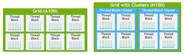
Thread block clusters and grids with clusters</em></p></figcaption></figure>

A grid is composed of thread blocks in the legacy CUDA programming model as in A100, shown in the left half of the diagram. The NVIDIA Hopper Architecture <mark style="color:yellow;">**adds an optional cluster hierarchy**</mark>, shown in the right half of the diagram.

### <mark style="color:green;">Asynchronous Execution Enhancements</mark>

The H100 introduces new features to improve asynchronous execution and enable further overlap of memory copies with computation and other independent work:

<mark style="color:blue;">**Tensor Memory Accelerator (TMA)**</mark>

The TMA is a new unit that efficiently transfers large blocks of data and multidimensional tensors *<mark style="color:yellow;">**between global memory and shared memory**</mark>*. It reduces addressing overhead and improves efficiency by supporting different tensor layouts, memory access modes, and reductions.

<mark style="color:blue;">**Asynchronous Transaction Barrier**</mark>

This new type of barrier counts both thread arrivals and transactions (byte counts).&#x20;

It allows *<mark style="color:yellow;">**threads to sleep until all other threads arrive**</mark>* and the sum of all transaction counts reaches an expected value, enabling more efficient synchronisation for asynchronous memory copies and data exchanges.

### <mark style="color:green;">**HBM3 Memory**</mark>

[<mark style="color:blue;">**HBM (High Bandwidth Memory)**</mark>](https://training.continuumlabs.ai/infrastructure/data-and-memory/high-bandwidth-memory-hbm3) is a type of high-performance memory that offers higher bandwidth and lower power consumption compared to traditional [<mark style="color:blue;">**GDDR memory**</mark>](#user-content-fn-3)[^3].&#x20;

[<mark style="color:blue;">**HBM3**</mark> ](https://training.continuumlabs.ai/infrastructure/data-and-memory/high-bandwidth-memory-hbm3)is the latest generation of this type of memory technology.

The H100 GPU comes with up to <mark style="color:yellow;">**80GB of HBM3 memory**</mark>, which is *<mark style="color:yellow;">**double the capacity of the A100's 40GB HBM2 memory**</mark>*.&#x20;

<mark style="color:blue;">**HBM3**</mark> provides a memory bandwidth of up to <mark style="color:yellow;">**3 terabytes per second (3 Tb/s)**</mark>, enabling fast data transfer between the GPU and memory, which is crucial for memory-intensive workloads like AI training and scientific simulations.&#x20;

To put this into perspective, <mark style="color:yellow;">**3 TB/s**</mark> is equivalent to transferring the entire content of a 1TB hard drive in just 0.33 seconds.

<figure><img src="https://1839612753-files.gitbook.io/~/files/v0/b/gitbook-x-prod.appspot.com/o/spaces%2FpV8SlQaC976K9PPsjApL%2Fuploads%2FuEFqowWbNEbCA9vRTVHJ%2Fimage.png?alt=media&#x26;token=dd66947a-86d4-45c2-8b81-6e0631b7ea15" alt=""><figcaption></figcaption></figure>

### <mark style="color:green;">**Multi-Instance GPU (MIG)**</mark>

<mark style="color:blue;">**MIG**</mark> was a feature first introduced in NVIDIA's Ampere architecture and further enhanced in the Hopper architecture.

It allows a single physical GPU to be <mark style="color:yellow;">**partitioned into multiple isolated instances**</mark>, each with its own dedicated resources, such as compute units, memory, and cache.

With MIG, the H100 GPU can be *<mark style="color:yellow;">**divided into up to seven independent instances**</mark>*, providing flexibility and efficiency in resource allocation.&#x20;

This feature is particularly useful in cloud and data centre environments, where *<mark style="color:yellow;">**multiple users or applications can share a single GPU**</mark>*, ensuring optimal utilisation and predictable performance.

MIG enables better resource management, improved security, and increased versatility in deploying GPU-accelerated workloads.

<figure><img src="https://1839612753-files.gitbook.io/~/files/v0/b/gitbook-x-prod.appspot.com/o/spaces%2FpV8SlQaC976K9PPsjApL%2Fuploads%2F4pjWUKKzx5j9Xiy7L9Aj%2Fimage.png?alt=media&#x26;token=b2ebdd55-de56-4ef7-ad92-5214ced33976" alt=""><figcaption><p>MIG can partition the GPU into as many as seven instances, each fully isolated with its own high-bandwidth memory, cache, and compute cores</p></figcaption></figure>

### <mark style="color:purple;">Let's review the specifications of the NVIDIA H100 GPU</mark>

### <mark style="color:green;">FP32 Performance</mark>

[<mark style="color:blue;">**FP32 (single-precision floating-point)**</mark>](#user-content-fn-4)[^4] performance measures the GPU's ability to perform single-precision arithmetic operations, commonly used in scientific simulations, computer graphics, and some AI workloads.&#x20;

<mark style="color:blue;">**TFLOPS (Tera Floating-Point Operations Per Second)**</mark> is a unit that represents the number of floating-point operations the GPU can perform per second.

The H100's <mark style="color:yellow;">**FP32 performance of 67 TFLOPS**</mark> is a substantial increase from the <mark style="color:yellow;">**A100's 19.5 TFLOPS**</mark>, indicating a significant boost in raw computational power.&#x20;

This high FP32 performance is for applications that require fast and precise single-precision calculations, enabling faster execution of complex simulations and rendering tasks.

### <mark style="color:green;">Tensor Performance</mark>

Tensor performance refers to the GPU's capability to *<mark style="color:yellow;">**perform mixed-precision matrix multiplication and convolution operations**</mark>*, which are the backbone of deep learning and AI workloads.&#x20;

FP16, bfloat16, and FP8 are <mark style="color:yellow;">**reduced-precision formats**</mark> that offer higher performance and memory efficiency compared to FP32.

The H100's tensor performance is groundbreaking, with up to <mark style="color:yellow;">**1,979 TFLOPS for FP16**</mark> <mark style="color:yellow;">**and bfloat16 operations**</mark>, and an massive <mark style="color:yellow;">**3,958 TFLOPS for FP8 operations**</mark>.&#x20;

This represents a massive leap from the A100's tensor performance, enabling faster training and inference of large-scale AI models.&#x20;

The support for lower-precision formats allows users to leverage the trade-off between precision and performance, achieving higher efficiency and faster results in AI workloads.

### <mark style="color:green;">**Memory Bandwidth**</mark>

Memory bandwidth is the rate at which data can be read from or written to the GPU's memory.&#x20;

It is measured in <mark style="color:blue;">**bytes per second (B/s)**</mark> and is a critical factor in determining the GPU's performance in memory-intensive workloads.

As highlighted, the H100's <mark style="color:blue;">**HBM3 memory subsystem**</mark> provides 3 TB/s of memory bandwidth, a significant improvement over the A100's 1.6 TB/s.&#x20;

This high memory bandwidth enables *<mark style="color:yellow;">**faster data transfer between the GPU and its memory**</mark>*, reducing latency and improving overall performance.&#x20;

It is particularly beneficial for workloads that involve large datasets, such as high-resolution video processing, scientific simulations, and training of complex AI models.

### <mark style="color:green;">**NVLink and PCIe Gen5**</mark>

[<mark style="color:blue;">**NVLink**</mark> ](https://training.continuumlabs.ai/infrastructure/servers-and-chips/nvlink-switch)is NVIDIA's proprietary *<mark style="color:yellow;">**high-speed interconnect technology**</mark>* that enables fast communication between GPUs in a <mark style="color:blue;">**multi-GPU system**</mark>.&#x20;

[<mark style="color:blue;">**PCIe (Peripheral Component Interconnect Express)**</mark>](https://training.continuumlabs.ai/infrastructure/networking-and-connectivity/pcie-peripheral-component-interconnect-express) is the standard interface for connecting GPUs to the CPU and other components in a computer system.

The H100 supports fourth-generation NVLink, providing up to <mark style="color:yellow;">**900 GB/s**</mark> of bidirectional bandwidth between two GPUs.

This high-speed interconnect enables efficient data exchange and collaboration between GPUs for scaling up multi-GPU systems.&#x20;

Additionally, the H100 supports [<mark style="color:blue;">**PCIe Gen5**</mark>](https://training.continuumlabs.ai/infrastructure/networking-and-connectivity/pcie-peripheral-component-interconnect-express), offering up to <mark style="color:yellow;">**128 GB/s**</mark> of bidirectional bandwidth, doubling the bandwidth of PCIe Gen4.&#x20;

This increased bandwidth *<mark style="color:yellow;">**allows for faster data transfer between the GPU and the CPU**</mark>*, reducing bottlenecks and enhancing overall system performance.

### <mark style="color:green;">TDP and Power Efficiency</mark>

<mark style="color:blue;">**TDP (Thermal Design Power)**</mark> is the *<mark style="color:yellow;">**maximum amount of heat the GPU is expected to generate under typical workloads**</mark>*, and it determines the cooling requirements for the system.&#x20;

Power efficiency refers to the GPU's ability to deliver high performance while consuming minimal power.

The H100's TDP <mark style="color:yellow;">**ranges from 300W to 700W**</mark>, depending on the specific model and cooling solution.&#x20;

While the higher TDP models offer the highest performance, they also require more advanced cooling solutions.&#x20;

The lower TDP models provide a balance between performance and power consumption, making them suitable for systems with limited power and cooling capacity.&#x20;

NVIDIA has made significant improvements in power efficiency with the Hopper architecture, enabling the H100 to deliver better performance per watt compared to previous generations.

In summary, the NVIDIA H100 GPU's specifications demonstrate its incredible computational power and memory capabilities.  A massive leap up from its predecessor, the A-100,

<details>

<summary><mark style="color:green;"><strong>Power Usage</strong></mark></summary>

\
To determine the power usage of the NVIDIA DGX H100 system, we need to consider the power specifications provided for its power supplies.

#### Power Specifications

* **Power Supply Units (PSUs)**: The system includes six power supplies.
* **Each Power Supply**:
  * **Wattage**: 3300 W (at 200-240 V, 16 A, 50-60 Hz)
  * **Total Power Consumption**: 10.2 kW max

Since the system is designed for redundancy, it operates with at least four PSUs actively supplying power. However, to calculate the maximum power usage, we'll consider all six PSUs.

#### Total Power Consumption Calculation

Each PSU provides 3300 W. With six PSUs:

$$Total Power Consumption=6×3300 W=19,800 WTotal Power Consumption=6×3300 W=19,800 W$$

In kilowatts, this is:

$$Total Power Consumption=19,800 W/1000=19.8 kWTotal Power Consumption=19,800 W/1000=19.8 kW$$

Thus, the NVIDIA DGX H100 system can consume up to 19.8 kW of power when all six power supplies are active and operating at maximum capacity.

#### Considerations for Power Usage

* **PSU Redundancy**: The system includes 4+2 redundancy, meaning it can continue to operate with up to two PSUs failing.
* **Operational Power**: The system is designed to function efficiently with at least four active PSUs. If fewer than four PSUs are operational, the system may operate at a reduced performance level or not boot at all.

#### Summary

The NVIDIA DGX H100 system has a maximum power consumption of <mark style="color:blue;">19.8 kW</mark> when all six power supplies are functioning at full capacity.&#x20;

This high power usage supports the system's advanced capabilities, including eight NVIDIA H100 GPUs, two Intel Xeon CPUs, and substantial memory and storage resources.

For more detailed information on the power specifications and other features of the NVIDIA DGX H100 system, refer to the official documentation provided by NVIDIA.

</details>

### <mark style="color:purple;">Integration with Other Technologies</mark>

The NVIDIA H100 GPU is integrated with various NVIDIA technologies and server solutions

### <mark style="color:green;">**NVIDIA AI Enterprise**</mark>

* NVIDIA AI Enterprise is a suite of software tools and frameworks optimised for AI workloads.
* It includes deep learning frameworks, <mark style="color:blue;">**CUDA-X libraries**</mark>, and <mark style="color:blue;">**NVIDIA's CUDA Toolkit**</mark>.
* The H100 GPU is fully supported by NVIDIA AI Enterprise, enabling development and deployment of AI applications.
* NVIDIA AI Enterprise simplifies the installation, management, and scaling of AI infrastructure, making it easier for organisations to adopt and use their H100 GPUs.

### <mark style="color:green;">**NVIDIA Magnum IO**</mark>

* Magnum IO is a suite of technologies that optimise I/O performance for accelerated computing.
* It includes [<mark style="color:blue;">**GPUDirect Storage (GDS)**</mark>](https://training.continuumlabs.ai/infrastructure/networking-and-connectivity/nvidia-gpudirect) and <mark style="color:blue;">**GPUDirect RDMA (Remote Direct Memory Access)**</mark>.
* GDS enables direct data transfer between storage and GPU memory, bypassing the CPU and reducing latency.
* GPUDirect RDMA allows direct data transfer between GPUs across different nodes, minimising data movement overhead.
* The H100 GPU leverages Magnum IO technologies to maximise I/O performance and efficiency in multi-node environments.

### <mark style="color:green;">**NVIDIA Quantum InfiniBand**</mark>

* NVIDIA [<mark style="color:blue;">**Quantum InfiniBand**</mark> ](#nvidia-quantum-infiniband)is a high-performance, low-latency networking solution for AI and HPC workloads.
* It enables fast communication between GPUs across multiple nodes, allowing efficient scaling of AI and HPC applications.
* The H100 GPU can be used with NVIDIA Quantum InfiniBand to create high-speed, low-latency clusters for distributed AI and HPC workloads.
* NVIDIA Quantum InfiniBand's high bandwidth and low latency complement the H100's computational power, enabling efficient scaling and faster time-to-solution.

### <mark style="color:green;">NVIDIA NVLink Switch System</mark>

* The [<mark style="color:blue;">**NVLink Switch System**</mark>](https://training.continuumlabs.ai/infrastructure/servers-and-chips/nvlink-switch) is a high-speed interconnect that allows multiple GPUs to communicate directly with each other.
* It enables up to 256 H100 GPUs to be connected in a high-speed, low-latency fabric.
* The NVLink Switch System provides a scalable infrastructure for AI and HPC workloads, allowing seamless scaling of H100 GPU clusters.
* With the NVLink Switch System, H100 GPUs can efficiently exchange data and collaborate on large-scale AI and HPC tasks, achieving massive parallelism and performance.

### <mark style="color:purple;">NVIDIA H100 Tensor Core GPU performance specifications</mark>

| Specification                  | H100 SXM                                                                                              | H100 PCIe                                           | H100 NVL1                                            |
| ------------------------------ | ----------------------------------------------------------------------------------------------------- | --------------------------------------------------- | ---------------------------------------------------- |
| FP64                           | 34 teraFLOPS                                                                                          | 26 teraFLOPS                                        | 68 teraFLOPS                                         |
| FP64 Tensor Core               | 67 teraFLOPS                                                                                          | 51 teraFLOPS                                        | 134 teraFLOPS                                        |
| FP32                           | 67 teraFLOPS                                                                                          | 51 teraFLOPS                                        | 134 teraFLOPS                                        |
| TF32 Tensor Core               | 989 teraFLOPS2                                                                                        | 756 teraFLOPS2                                      | 1,979 teraFLOPS2                                     |
| BFLOAT16 Tensor Core           | 1,979 teraFLOPS2                                                                                      | 1,513 teraFLOPS2                                    | 3,958 teraFLOPS2                                     |
| FP16 Tensor Core               | 1,979 teraFLOPS2                                                                                      | 1,513 teraFLOPS2                                    | 3,958 teraFLOPS2                                     |
| FP8 Tensor Core                | 3,958 teraFLOPS2                                                                                      | 3,026 teraFLOPS2                                    | 7,916 teraFLOPS2                                     |
| INT8 Tensor Core               | 3,958 TOPS2                                                                                           | 3,026 TOPS2                                         | 7,916 TOPS2                                          |
| GPU memory                     | 80GB                                                                                                  | 80GB                                                | 188GB                                                |
| GPU memory bandwidth           | 3.35TB/s                                                                                              | 2TB/s                                               | 7.8TB/s3                                             |
| Decoders                       | 7 NVDEC 7 JPEG                                                                                        | 7 NVDEC 7 JPEG                                      | 14 NVDEC 14 JPEG                                     |
| Max thermal design power (TDP) | Up to 700W (configurable)                                                                             | 300-350W (configurable)                             | 2x 350-400W (configurable)                           |
| Multi-instance GPUs            | Up to 7 MIGs @ 10GB each                                                                              | Up to 7 MIGs @ 10GB each                            | Up to 14 MIGs @ 12GB each                            |
| Form factor                    | SXM                                                                                                   | PCIe > dual-slot > air-cooled                       | 2x PCIe > dual-slot > air-cooled                     |
| Interconnect                   | NVLink: > 900GB/s PCIe > Gen5: 128GB/s                                                                | NVLink: > 600GB/s PCIe > Gen5: 128GB/s              | NVLink: > 600GB/s PCIe > Gen5: 128GB/s               |
| Server options                 | NVIDIA HGX™ H100 partner and NVIDIA- Certified Systems™ with 4 or 8 GPUs NVIDIA DGX™ H100 with 8 GPUs | Partner and NVIDIA- Certified Systems with 1–8 GPUs | Partner and NVIDIA- Certified Systems with 2-4 pairs |
| NVIDIA Enterprise Add-on       | Included                                                                                              | Included                                            |                                                      |

* H100 SXM: Uses the SXM (Scalable Link Interface) form factor.
* H100 PCIe: Uses the PCIe (Peripheral Component Interconnect Express) form factor with a dual-slot, air-cooled design.
* H100 NVL1: Uses two PCIe cards with a dual-slot, air-cooled design.

### <mark style="color:purple;">Explanation of IEE standard</mark>

The IEEE 754 standard, officially known as IEEE Standard for Floating-Point Arithmetic, is a <mark style="color:yellow;">technical standard for floating-point computation</mark> established by the <mark style="color:blue;">**Institute of Electrical and Electronics Engineers (IEEE)**</mark>.&#x20;

The standard was first published in 1985 and has since undergone revisions to include more features and accommodate advancements in computing technology.  The most significant revisions were made in 2008, and it's often referred to based on this version as IEEE 754-2008.

#### <mark style="color:green;">Purpose of IEEE 754</mark>

The primary goal of IEEE 754 is to provide a <mark style="color:yellow;">uniform standard for floating-point arithmetic</mark>.&#x20;

Before this standard, many different floating-point implementations could lead to discrepancies in calculations across different systems. This variability was problematic, especially for applications requiring consistent and reliable results, such as scientific computations.&#x20;

IEEE 754 addresses these issues by defining:

<mark style="color:green;">**Formats for Number Representation**</mark>

* <mark style="color:blue;">**Binary formats:**</mark> These include single precision (32-bit), double precision (64-bit), and extended precision (which can be 80-bit or more).
* <mark style="color:blue;">**Decimal formats:**</mark> Introduced in the 2008 revision, these are useful in financial computations where decimal rounding precision is required.

<mark style="color:green;">**Arithmetic Operations**</mark>

* The standard specifies the results of arithmetic operations like addition, subtraction, multiplication, division, square root, and remainder. It also includes rounding rules and handling of exceptional cases like division by zero and overflow.

<mark style="color:green;">**Rounding Rules**</mark>

* IEEE 754 defines several rounding modes to nearest value, towards zero, and towards positive or negative infinity. This is crucial for ensuring that floating-point operations can be consistently replicated across different computing platforms and environments.

<mark style="color:green;">**Handling of Special Cases**</mark>

* The standard provides a detailed mechanism for dealing with special values like infinity (positive and negative), NaNs (Not a Number), and denormalised numbers. Handling these special cases ensures that the floating-point operations do not crash unexpectedly and provide meaningful outputs even under exceptional conditions.

#### <mark style="color:green;">Key Features of IEEE 754</mark>

* <mark style="color:blue;">**Normalised and Denormalised Numbers:**</mark> Normalised numbers have a normalised mantissa where the most significant digit is non-zero. Denormalised numbers allow for representation of numbers closer to zero than would otherwise be possible with normalised representations.
* <mark style="color:blue;">**Special Numbers:**</mark>
  * **Infinities:** Positive and negative infinities are used to represent results of operations that exceed the maximum representable value.
  * **NaN (Not a Number):** Used to represent undefined or unrepresentable values, such as $$0/00/00/0$$ or the square root of a negative number.
  * **Zero:** IEEE 754 makes a distinction between positive and negative zeros, which can be relevant in certain mathematical operations.

#### <mark style="color:green;">Impact of IEEE 754</mark>

The adoption of IEEE 754 has had a profound impact on the reliability and portability of software:

* <mark style="color:blue;">**Consistency:**</mark> Programs that use IEEE 754 floating-point arithmetic can expect consistent results across compliant systems, crucial for software portability and reproducibility of results.
* <mark style="color:blue;">**Optimisation:**</mark> Hardware manufacturers have optimised their processors to efficiently handle IEEE 754 operations, leading to improved performance of applications relying on floating-point calculations.
* <mark style="color:blue;">**Software Development:**</mark> The clear rules and definitions provided by IEEE 754 have simplified the development of numerical applications, as developers can rely on standardized behavior of floating-point arithmetic.

Overall, IEEE 754 continues to be a fundamental standard in the computing world, particularly valuable in fields like scientific computing, engineering, and finance, where precision and correctness of numerical computations are critical.

### <mark style="color:purple;">The components of the floating-point representation of numbers</mark>

The terms **mantissa**, **exponent**, and **sign bit** are components of the floating-point representation of numbers, as defined by the IEEE 754 standard for floating-point arithmetic.&#x20;

Each of these components plays a role in how numbers are stored and processed in computers, particularly in the area of scientific calculations where a wide range of values and precision is necessary.&#x20;

Let’s explore each of these components:

#### <mark style="color:green;">**Mantissa (Significand)**</mark>

The mantissa, also <mark style="color:yellow;">**known as the significand**</mark>, is the part of a floating-point number that contains its significant digits. In the context of the binary systems used in computers:

* <mark style="color:blue;">**Function**</mark><mark style="color:blue;">:</mark> The mantissa represents the precision of the number and essentially carries the "actual" digits of the number. For a given floating-point number, the mantissa represents the number's digits in a scaled format.
* <mark style="color:blue;">**Details**</mark><mark style="color:blue;">:</mark> In a normalised floating-point number, the mantissa is adjusted so the first digit is always a 1 (except in the case of denormalised numbers, where it can be 0). This digit is not stored (known as the "hidden bit" technique) in many floating-point representations to save space, effectively giving an extra bit of precision.

<figure><img src="https://1839612753-files.gitbook.io/~/files/v0/b/gitbook-x-prod.appspot.com/o/spaces%2FpV8SlQaC976K9PPsjApL%2Fuploads%2FTEygvptfickW3LmIcMBa%2Fimage.png?alt=media&#x26;token=764ac4d7-7046-445a-b2a6-d54d2c866f3f" alt=""><figcaption></figcaption></figure>

#### <mark style="color:green;">**Exponent**</mark>

The exponent in a floating-point representation <mark style="color:yellow;">scales the mantissa</mark> to provide a very large or very small range of values.

* <mark style="color:blue;">**Function**</mark><mark style="color:blue;">:</mark> The exponent determines the scale of the number, effectively shifting the decimal (or binary) point to the right or left. This allows floating-point formats to represent very large or very small numbers compactly.
* <mark style="color:blue;">**Details**</mark><mark style="color:blue;">:</mark> The exponent is stored with a bias in binary systems. For example, an 8-bit exponent in IEEE 754 single-precision floating-point format is stored with a bias of 127.  The actual exponent value is calculated by subtracting 127 from the stored exponent value. This bias allows the representation of both positive and negative exponents.

#### <mark style="color:green;">**Sign Bit**</mark>

The sign bit is the simplest of the three; it indicates the sign of the number.

* <mark style="color:blue;">**Function**</mark><mark style="color:blue;">:</mark> It tells whether the number is positive or negative.
* <mark style="color:blue;">**Details**</mark><mark style="color:blue;">:</mark> In floating-point formats, a sign bit of 0 usually represents a positive number, and a sign bit of 1 represents a negative number.

#### <mark style="color:purple;">Example in Context:</mark>

Consider a <mark style="color:yellow;">32-bit single-precision floating-point number</mark> under IEEE 754:

* **Sign bit**: 1 bit
* **Exponent**: 8 bits (with a bias of 127)
* **Mantissa**: 23 bits (plus 1 hidden bit)

For example, a binary floating-point number could look something like this:

* **Sign bit**: 0
* **Exponent**: 10000001 (which represents 129 in decimal; with bias subtracted, it becomes $$129−127=2129 - 127 = 2129−127=2$$)
* **Mantissa**: 10100000000000000000000 (where the leading 1 is the hidden bit)

This number represents $$1.10100000000000000000000 \times 2^2$$ in binary, which translates into a decimal number after calculating the binary to decimal conversion of the mantissa and applying the exponent as the power of two.

Understanding these components is fundamental for software development and hardware design involving floating-point arithmetic, ensuring precise and efficient numerical computations.

### <mark style="color:purple;">Number types</mark>

#### <mark style="color:blue;">**Peak FP64**</mark>

* **Definition**: This is the maximum number of double-precision floating-point operations per second, measured in teraflops (TFLOPS). <mark style="color:yellow;">Double precision</mark> (64-bit) offers high accuracy by using 52 bits for the mantissa, 11 bits for the exponent, and 1 sign bit.
* **Importance**: It is crucial for scientific computing and engineering simulations that require high numerical precision to ensure the correctness of results.

#### <mark style="color:blue;">**Peak FP64 Tensor Core**</mark>

* **Definition**: This measures the same as Peak FP64 but specifically using the Tensor Cores, specialised processing units within NVIDIA GPUs designed to accelerate deep learning tasks.
* **Importance**: Provides enhanced performance for certain types of calculations, such as those involving matrices and deep learning models, leveraging optimised hardware.

#### <mark style="color:blue;">**Peak FP32**</mark>

* **Definition**: The maximum number of single-precision floating-point operations per second. Single precision (32-bit) uses 23 bits for the mantissa, 8 bits for the exponent, and 1 sign bit.
* **Importance**: Balances precision and performance. It is widely used in gaming, graphics rendering, and machine learning where high precision is less critical than performance.

#### <mark style="color:blue;">**Peak FP16**</mark>

* **Definition**: The maximum number of half-precision floating-point operations per second. Half precision (16-bit) allocates 10 bits to the mantissa, 5 bits to the exponent, and 1 sign bit.
* **Importance**: Offers a good compromise between storage space and precision, suitable for mobile devices, image processing, and certain types of machine learning models where high precision is less necessary.

#### <mark style="color:blue;">**Peak BF16**</mark>

* **Definition**: The maximum number of bfloat16 floating-point operations per second. Bfloat16 is a truncated floating point format that uses the same 8-bit exponent as FP32 but with a shorter 7-bit mantissa.
* **Importance**: Particularly useful in machine learning and deep learning, providing near-single precision range with reduced precision, which is typically sufficient for these applications.

#### <mark style="color:blue;">**Peak TF32 Tensor Core**</mark>

* **Definition**: This is a specialised metric for the performance of Tensor Float 32 operations per second using Tensor Cores. TF32 is designed to provide the range of FP32 operations while delivering the performance of FP16.
* **Importance**: Critical for AI training tasks, offering a balance of performance and accuracy, enhanced by hardware acceleration.

#### <mark style="color:blue;">**Peak FP16 Tensor Core**</mark>

* **Definition**: Measures the performance of half-precision operations using Tensor Cores, potentially with and without the use of Sparsity.
* **Importance**: Enhances the computational speed for tasks that can tolerate reduced precision, with sparsity providing additional performance gains by skipping zero values in data.

#### <mark style="color:blue;">**Peak BF16 Tensor Core**</mark>

* **Definition**: Similar to Peak BF16 but specifically using Tensor Cores, again with potential variations for sparsity.
* **Importance**: Optimises performance for AI workloads, allowing for faster training times and efficient model deployment.

#### <mark style="color:blue;">**Peak FP8 Tensor Core**</mark>

* **Definition**: This measures the performance of 8-bit floating-point operations per second using Tensor Cores, designed to provide even lower precision with extremely high throughput.
* **Importance**: Useful in scenarios where ultra-high volume computations with lower accuracy requirements are needed, such as certain inference tasks in deep learning.

#### <mark style="color:blue;">**Peak INT8 Tensor Core**</mark>

* **Definition**: The maximum number of 8-bit integer operations per second using Tensor Cores. This format is common in deep learning inference where high precision is not necessary.
* **Importance**: Allows for rapid computation in large-scale and real-time applications, like video processing and real-time AI services, with significant acceleration when using sparsity.

Each of these performance metrics highlights a trade-off between precision and speed, where the choice of number type depends on the specific requirements of the application, such as the need for accuracy versus the need for fast processing and reduced memory usage.

[^1]: Genome sequencing involves analysing the sequences of nucleotides in DNA to identify and map all the genes of an organism. The Smith-Waterman algorithm is a dynamic programming algorithm used for local sequence alignment, helping in the identification of similar regions between two DNA or protein sequences. With the acceleration provided by DPX instructions, the Smith-Waterman algorithm can process larger sequences more efficiently

[^2]: Robotics relies on algorithms like Floyd-Warshall for optimal route finding to navigate robots efficiently within their environment. The Floyd-Warshall algorithm is used to find the shortest paths in a weighted graph with positive or negative edge weights (but with no negative cycles). This is critical for robotics applications that require path optimisation in real-time, such as autonomous vehicle navigation and warehouse robotics.

[^3]: GDDR memory, short for <mark style="color:yellow;">**Graphics Double Data Rate memory**</mark>, is a type of <mark style="color:blue;">**DRAM**</mark> specifically designed for use in graphics cards and gaming consoles to accelerate graphics rendering. Compared to traditional DDR memory found in most computers, GDDR memory offers higher bandwidth and speed, which allows for faster loading and smoother performance in visual applications like video games and 3D rendering.&#x20;

[^4]: Floating Point Precision is a representation of a number through binary.  FP32 or single precision 32-bit floating point precision uses 32 bits of binary to represent numbers. This format is the most widely used floating point precision format that adequately trades some precision for a lighter weight value represented with less digits. Less digits take up less memory which in turn increases speed.\
    \
    &#x20;&#x20;


---

# Agent Instructions: Querying This Documentation

If you need additional information that is not directly available in this page, you can query the documentation dynamically by asking a question.

Perform an HTTP GET request on the current page URL with the `ask` query parameter:

```
GET https://training.continuumlabs.ai/infrastructure/servers-and-chips/the-nvidia-h100-gpu.md?ask=<question>
```

The question should be specific, self-contained, and written in natural language.
The response will contain a direct answer to the question and relevant excerpts and sources from the documentation.

Use this mechanism when the answer is not explicitly present in the current page, you need clarification or additional context, or you want to retrieve related documentation sections.
